
EV charging is scaling quickly, and the electronics inside each charger must keep pace. The International Energy Agency’s Global EV Outlook 2024 reports that public charging points exceeded four million worldwide in 2023, rising about 40% in one year. Public fast chargers grew even faster, by roughly 55%. These figures describe infrastructure, not PCB demand directly. Still, they show why dependable power electronics matter.
EV Charging Module PCB Design is the engineering of circuit boards that support power conversion, control, protection, and communication within a charging module. A designer must consider high-current copper paths, component spacing, heat removal, switching noise, and reliable connections. A few millimeters can affect insulation or routing choices. Heat is tangible: a power component can warm its nearby board, connector, and enclosure. Small details count.
The design also depends on the charger’s power level, topology, cooling method, and manufacturing process. A board suited to one module may not fit another. Engineers often balance efficiency, safety, serviceability, cost, and production yield rather than optimize one figure alone. Standards and verification testing should guide design decisions; a visually clean layout is not proof of reliable operation. That distinction is easy to miss. This introduction examines the practical choices behind EV charging module boards, from electrical and thermal planning to testing and manufacturability. The evidence is useful, but no single layout solves every charger. Real hardware can expose assumptions that looked reasonable on screen.
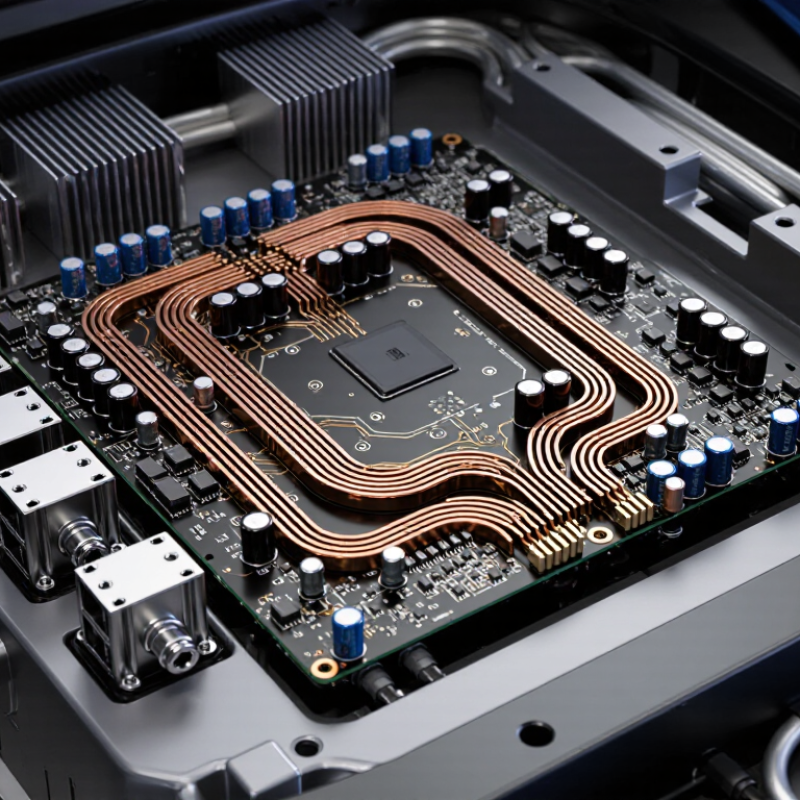
An EV charging module PCB is the circuit board that helps a charger convert and control electrical power. It is not the entire charging station. Depending on the charger design, the board may support power conversion, switching, sensing, and communication with the vehicle. Small sensors can monitor current, voltage, and temperature, while control circuits adjust power delivery or trigger a shutdown when readings exceed safe limits. That distinction matters.
The IEA’s Global EV Outlook 2024 counted over four million public charging points worldwide in 2023, roughly 40% more than in 2022. Fast chargers grew by about 55%. More charging equipment means more demand for dependable electronics, but a PCB cannot solve every system-level problem. Designers must consider heat near power components, electrical noise, and the physical spacing needed for insulation. A temperature sensor placed too far from a hot component may report a reassuring number that misses a local hotspot. Heat is unforgiving. Engineers test boards under realistic loads, then revise layouts when measurements disagree with simulations. The process is rarely perfect on the first pass. A sound module PCB balances efficiency, protection, serviceability, and cost for its specific charger architecture.
An EV charging module PCB must route energy and coordinate decisions within a compact space. Its power circuit carries current through switching devices, conversion stages, and output connections. The exact arrangement depends on the charger’s architecture. Control circuits monitor voltage, current, and temperature, then adjust switching signals as conditions change. A current sensor, for example, can help the controller detect an unexpected load. Heat is physical.
The two circuit groups must work together without interfering with each other. A control signal may be small, but it can command a device handling substantial power. Designers therefore consider electrical isolation, grounding, clearances, and the placement of sensitive signal traces. Short, direct gate-drive paths can help reduce switching noise. Copper thickness and board area affect heat spreading, too. A warm connector near a temperature sensor can distort readings if placement is careless. That detail is easy to underestimate.
Testing should reflect real operating conditions, including changing loads and temperature. Measurements from prototypes can reveal noise or hot spots that a schematic cannot show. Even a well-reviewed layout can have awkward trade-offs between compactness, cooling, and separation. The first revision is rarely perfect.
What Is EV Charging Module PCB Design?
EV charging module PCB design arranges the power-conversion and control circuits that move energy safely from the supply to a vehicle. Typical components include power switches, gate drivers, control processors, voltage and current sensors, isolation circuits, and protection devices. Their placement matters: a compact switching loop can reduce electrical noise, while separated high- and low-voltage areas help preserve isolation. Small layout choices carry real consequences.
Electrical requirements depend on the charger’s voltage, current, cooling method, and operating environment. Copper thickness and trace geometry must handle current without excessive heating. Designers also check creepage, clearance, insulation, and thermal limits against applicable standards, including IEC 60664-1. The International Energy Agency’s Global EV Outlook 2024 reported more than four million public charging points worldwide by the end of 2023. That growth makes dependable, serviceable power electronics increasingly important. Extra copper can spread heat, but it also changes parasitic effects; a calculation alone may not capture the final enclosure’s behavior.
Tips: Keep switching paths short, place sensors away from noisy nodes, and provide clear test points. Validate the assembled board under realistic load and temperature conditions. A neat schematic is not proof of a robust layout.
This overview focuses on a typical onboard charger (OBC) power-conversion module. An off-board DC fast charger has a different power-stage architecture. Values and design choices depend on the vehicle, power level, operating environment, and applicable regulations.
| Design area | Key component(s) | Purpose | Electrical and PCB design requirements | Typical verification |
|---|---|---|---|---|
| AC input and protection | Input connector, fuse, surge suppression, EMI filter, inrush-limiting circuit | Accepts grid power and helps protect the charger from surges, conducted noise, and excessive startup current. | Size conductors and protection for the specified input voltage, current, fault conditions, and temperature rise. Keep noisy switching paths away from sensitive control and sensing circuits. | Input-current, inrush, surge-immunity, and conducted-emissions tests. |
| Rectifier and power-factor correction | Rectifier stage and PFC switching devices, inductors, and capacitors | Converts AC to a regulated DC link and, in many OBC designs, improves input power factor and controls input-current harmonics. | Design switching-current loops with low parasitic inductance. Select voltage-rated parts with appropriate ripple-current, transient, and thermal margins. Coordinate the control scheme with the DC-link operating range. | Power-factor and harmonic measurements, efficiency, ripple, and switching-waveform checks. |
| DC-link energy storage | High-voltage capacitors, discharge path, and DC-link sensing network | Buffers energy between conversion stages and supports stable operation during input and load changes. | Account for DC voltage, ripple current, lifetime, and stored-energy hazards. Provide suitable spacing, discharge provisions, and measurement circuitry for the actual circuit voltage. | DC-link ripple, startup and shutdown behavior, discharge time, and capacitor temperature. |
| Isolated DC/DC conversion | Power switches, transformer, resonant or clamping components, and secondary rectification | Transfers power from the DC link to the vehicle battery while providing the required voltage conversion and galvanic isolation. | Meet the required isolation and insulation coordination. Keep primary and secondary circuits separated according to the applicable working voltage, transient level, material group, pollution degree, and altitude. | Isolation, dielectric-strength, efficiency, output-regulation, and load-transient tests. |
| Gate drive and switching control | Gate-driver circuits, gate resistors, isolated supplies, and controller | Controls power-device switching and supports protection functions such as overcurrent and undervoltage response. | Place drivers close to their switches, minimize gate-loop area, manage return paths, and control switching edges to balance losses, overshoot, and electromagnetic interference. | Gate-voltage and switching-node waveform checks, protection-response tests, and EMI evaluation. |
| Current, voltage, and temperature sensing | Current sensors or shunts, voltage dividers, temperature sensors, and signal-conditioning circuits | Provides feedback for regulation, monitoring, and fault shutdown. | Route low-level signals away from high-current switching nodes. Use suitable filtering, Kelvin connections where needed, and isolation when required by the safety architecture. | Measurement accuracy across operating range, noise susceptibility, calibration, and fault detection. |
| PCB layout and insulation | Copper layers, power planes, isolation barriers, slots, and board materials | Carries power safely while limiting parasitic effects, electrical stress, and unintended coupling. | Determine trace width, copper weight, spacing, creepage, and clearance from current, temperature rise, working voltage, transients, board material, and environment. Do not rely on a single generic spacing value. | Design-rule review, thermal assessment, insulation review, and prototype layout validation. |
| Thermal management | Heat spreaders, thermal vias, interface materials, and temperature monitoring | Moves heat from semiconductors and passive components to the enclosure or cooling system. | Estimate losses at worst-case operating conditions and keep component junction and board temperatures within rated limits. Consider airflow or liquid-cooling interfaces where specified. | Temperature-rise and thermal-soak tests under defined load and ambient conditions. |
| Standards and system integration | Safety, EMC, charging-control, and vehicle-interface design provisions | Ensures the module can be assessed as part of the complete charging and vehicle system. | Identify applicable requirements early. Relevant standards may include IEC 61851 for conductive charging systems, IEC 62477-1 for power electronic converter safety, and IEC 60664-1 for insulation coordination; applicability depends on product scope and jurisdiction. | System-level safety, EMC, charging-interface, and regulatory compliance assessment. |
Design note: Final component ratings, PCB dimensions, isolation distances, and test limits should be established from the product specification, the selected topology, applicable standards and their current editions, and the intended operating environment.
What Is EV Charging Module PCB Design?
Steps in Designing the PCB Layout
Begin with the module’s electrical and mechanical requirements. Record the operating voltage, peak current, connector positions, board dimensions, and available cooling. These details guide component placement and copper sizing. Mark high-voltage areas and keep sensitive control circuits away from noisy switching paths. Check the required isolation distances against applicable standards and the product specification.
Place power components near their connectors to shorten high-current paths. Keep gate-drive and sensing traces compact, and provide a clear return path for each signal. Use suitably wide copper for power routes, then add thermal vias beneath hot components when the board stack-up permits. Separate power and control grounds thoughtfully; a split that looks tidy can still create unwanted noise. Run design-rule checks, inspect clearances, and review heat flow before ordering a prototype. Measure the finished board under realistic load, since calculations alone can miss local hotspots.
Tips: Keep a current-path sketch beside the layout. Check connector access in the enclosure. Leave room for measurement probes. Revisit assumptions after thermal testing. One detail is easy to overlook: test points can crowd an otherwise clean layout.
A typical sequence of steps, from defining requirements to validating the finished layout.
The numbered values indicate workflow order only; they do not represent time, cost, or performance. Actual design processes vary by charger architecture and project requirements.
An EV charging module PCB must manage high current, switching noise, heat, and fault signals on a compact board. Testing should begin with visual inspection and electrical checks, then move to insulation resistance, dielectric withstand, and temperature-rise tests. Verify protection circuits under realistic fault conditions, not only on a bench supply. Small defects matter. A poorly soldered power connection can heat locally, even when the overall board temperature looks acceptable.
The IEA’s Global EV Outlook 2024 reports that public charging points grew by about 40% in 2023, with fast chargers growing faster than slower units. That expansion raises the value of repeatable production. Use controlled solder profiles, documented component substitutions, and traceable test records. IPC-A-610 workmanship criteria and IEC 61851-1 safety requirements can help shape inspection and verification plans. They do not replace product-specific engineering review.
Thermal cycling and vibration tests can expose cracked joints or connector movement before field deployment. Check creepage and clearance against the actual voltage, insulation material, and pollution conditions. Heat leaves clues. A thermocouple near a switching device may reveal a hotspot hidden by an enclosure sensor. Production sampling also has limits; a passing sample cannot prove every board is sound. Test coverage should target likely failure paths, then be revised when field returns or process changes reveal gaps.
